At Teledyne ICM, we offer digital radiography detectors from two distinct families: CMOS technology detectors and aSi technology detectors. Understanding the disparities between these two technologies is crucial for selecting the ideal solution to meet your specific inspection requirements. In this article, we delve into the characteristics, advantages, and applications of both CMOS and aSi detectors to aid in your decision-making process.
Advantages of CMOS and aSi detectors
aSi technology detectors
- Detector active area: these detectors boast larger active areas, facilitating the inspection of bigger-sized parts with ease.
- High image quality: particularly at high X-ray doses, is achieved through a combination of lower resolution and thicker scintillator.
- Gamma energy compatibility: compatible with gamma energy sources such as Ir192 & Se75, enhancing versatility in inspection applications.
- Value proposition: the cost-to-size ratio is favorable.
CMOS technology detectors
- Real-time imaging: capable of real-time imaging at over 90 fps, even at full resolution, facilitated by high-speed integrated circuits.
- Low X-ray dose imaging: achieves high image quality at low X-ray doses, thanks to the low noise characteristics inherent in CMOS technology.
- Enhanced resolving power: small pixel sizes, combined with high fill factor and sensitivity, result in increased resolving power (MTF), ensuring intricate details are captured effectively.
- Artifact-free imaging: absence of image lag, ghosting, offset drift, or other artifacts owing to the high electron mobility and superior quality of the CMOS fabrication process.
Applications of CMOS & aSi detectors
aSi technology detectors:
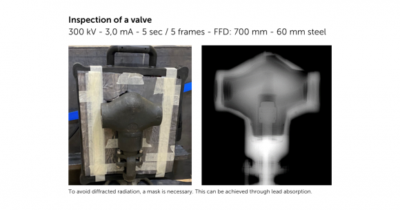
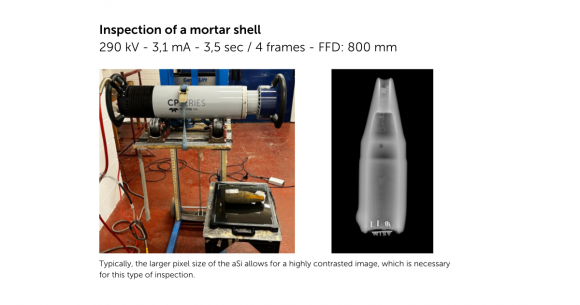
Inspection of larger thicknesses
Radiography of high thickness materials can be challenging due to the high energy required. The larger pixel size of the aSi allows for a highly contrasted image, which is necessary for this type of inspection.
Examples of inspections of larger thicknesses
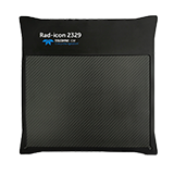
For those examples, we used the Go-Scan 4335.
CMOS technology detectors:
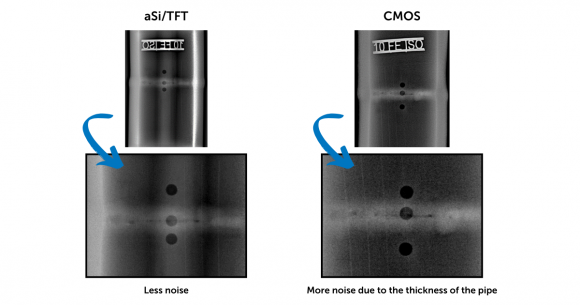
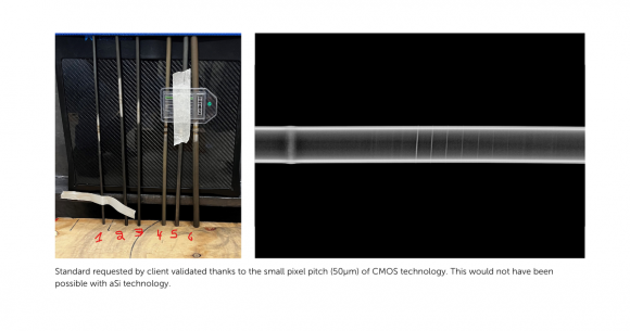
Inspection of small thicknesses (from 0,5 to 6 mm)
The small pixel pitch (50 µm) of CMOS technology ensures high image quality when inspecting small thicknesses.
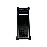
For this example, we used the Go-Scan 2329.
Corrosion Under Insulation (CUI) and real time imaging
CMOS technology offers real-time imaging and achieves high image quality at low X-ray doses, which is perfectly suited for hand-held inspections of insulated pipes.
For this example, we used the Go-Scan C-View.
In conclusion, while both CMOS and aSi technology detectors offer unique advantages, the choice ultimately depends on the specific requirements of your NDT inspection tasks.
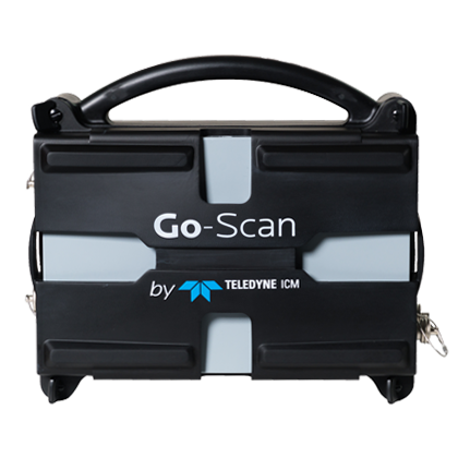
At Teledyne ICM, we have a wide range of CMOS and aSi digital detectors to suit all your applications:
Take a look at our Go-Scan series, and don’t hesitate to contact us if you need more information.